Wizard
@0FC7.ADF - Wizard
Attached Processor
I0FC7.ADF -
Init file for @0FC7.ADF
ADF Sections (all three of them..)
189-186
Wizard Adapter and Wizard Memory Expansion Ooption
GRIDNET: Natural
Gas Operations Optimizing System
Wizard Adapter PN 34F3062
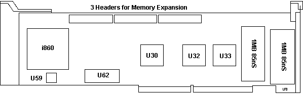
U30 IBM I0120006
U32 IBM I0142101
U33 IBM I0122188 |
U59 32.000 MHz osc
U62 D27C512 EPROM (BIOS)
|
RAM, right bank, Toshiba, 511002AZ-80
left bank Mitsubishi, M5M41002AL-80
Wizard Memory Expansion Option PN
34F3061
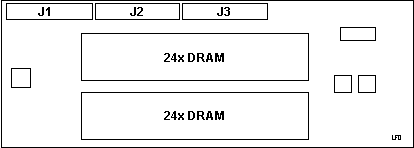
Each bank of 24x DRAM modules equals 3MB, so the adapter adds 6MBs to
the Wizard.
Original images from Dan Snyder
The i860 microprocessor (announced
by Intel on February 27, 1989) is a RISC integer core and contains an advanced
floating point processor, a graphics unit and internal instruction and
data cache integrated in a single one-million transistor chip.
The Wizard Adapter contains 2MB of DRAM (85ns).
The application or subroutine running on the Wizard resides in this on-card
memory. Users with application requirements greater than 2MB need
the Wizard Memory Expansion Option adapter. This adapter attaches
to the Wizard Adapter and
provides an additional 6MB of memory, for a maximum of 8MB.
The Wizard operates under OS/2
Standard Edition Version 1.1 and OS/2 Extended Edition Version 1.1, and
later versions, through the use of application device drivers shipped with
this product. These drivers control the use of the i860 processor
and provide interface functions to the 80386/80486.
In order to take advantage of
the Wizard Adapter, applications must be recompiled to run with the i860
processor, using the Intel i860 Microprocessor OS/2 Software Development
Tools. These tools include a Simulator Linker, Assembler, Debugger,
C Compilers and Libraries. This toolkit is available through IBM
(refer to Programming Announcement 289-638, dated November 14, 1989).
Intel intends to provide a FORTRAN Toolkit (including FORTRAN Vectorizer)
for OS/2 FORTRAN application.
The IBM PS/2 Model 80-111 and 80-311 require planar EC
C00835 in order to operate with the IBM PS/2 Wizard Adapter. Customers
with PS/2 Model 80-111 with serial numbers 72-6000000 through 72-6039999
or PS/2 Model 80-311 with serial numbers 72-65000000 through 72-6509999
should contact their IBM representative or authorized dealer for information
on obtaining this
modification. (Ed. I think these
are the non-busmaster compatible planars)
Initially supported products:
- PS/2 Model 70 or Model 80. NOTE:
The Model P70 is not supported.
Power Requirements Due to
power requirements, the user must dedicate two full expansion slots to
accommodate the Wizard Adapter. If the user has installed both the
Wizard Adapter and the Wizard Memory Expansion Option, the two allocated
slots will be sufficient.
Dan sent this as well-
i860 Overview
Jan Gray uunet!microsoft!jangr Microsoft Corp., Redmond
Wash. 206-882-8080. Any typos/misinterpretations are my own.
I speak only for myself.
(what I consider interesting features of the part), taken from the "i860(tm)
64-bit Microprocessor Programmer's Reference Manual", Order Number 240329-001,
(C) Intel Corp. 1989.
Overview
* 64 bit external data/instruction bus
* 128 bit on-chip data bus
* 64 bit on-chip instruction bus
* 8K data cache, virtual addressed, write-back, two-way "set associative",
2x128 lines of 32 bytes
* 4K instruction cache, virtual addressed
* 64 entry TLB
* core integer RISC unit
* floating-point unit with pipelined multiply and add units (can also
be used "unpipelined")
* some multiply-accumulate type floating point instructions
* dual instruction mode can simultaneously dispatch a 32-bit core instruction
and a 32-bit floating-point instruction
Data Types
* BE bit in epsr (extended processor status register) selects big/little
endian format in memory, instructions always little-endian
* 32 bit signed/unsigned integers
* IEEE 754 format single (32-bit) and double (64-bit) precision floating
point numbers
* pixels:
* stored as 8, 16, or 32 bits (always operates on 64 bits of pixels
at a time)
* colour intensity shading instructions treat divide pixels
into fields:
pixel size colour 1 bits colour
2 bits colour 3 bits other bits
8
....................N........................ 8 - N
16
6
6
4
0
32
8
8
8
8
[These particular field assignments are a result of the pixel add instructions
described below.]
Memory Management
* NO SEGMENTS!
* 32 bit virtual addresses (translation can be disabled)
* translated identically to 386 virtual address: two level address
translation, with bits 31..20 of address selecting:
* dirbase register specifies page directory
* 1st level: addr[31..22] specifies page directory entry, yielding
permissions and address of the second level page
table
* 2nd level: addr[21..12] specifies page table entry, yielding
additional
permissions and address of the physical page
* addr[11..0] specifies byte offset within physical page
(4K pages)
* page table bits:
* P - page is present
* CD - cache disable: page is not cacheable
* WT - page is write-through. disables internal caching.
Either CD or WT can be passed through to the external PTB pin, depending
upon PBM bit in epsr.
* U - user: if 0, page in inaccessible in user mode.
* W - writable: if 0, page is not writable in user mode,
and may be writable in supervisor mode depending upon WP bit in epsr.
* A - accessed: automatically set first time page is accessed
* D - dirty: traps when D=0 and page is written
* two bits reserved, three bits user-definable
* page directory PTE bits and second level PTE bits are combined
in the most restrictive fashion
* 64 entry TLB
Caches
* Flush instruction forces a dirty data cache line (32 bytes) back
to memory. Intel supplies suggested code to flush entire data cache.
* Storing to dirbase register with ITI bit set invalidates TLB and
instruction caches; must flush data cache first! [Remember, the data
cache is virtually addressed.]
Core Unit
* Standard 32 bit RISC architecture:
* 32 32-bit integer registers
* fault instruction, psr, epsr, dirbase, data breakpoint registers
* r0 always reads as 0
* 8, 16, 32 bit integer load/store insns, operands must be appropriately
aligned; byte or word values are sign extended on load. [I hope you
don't use "unsigned char" too much...]
* 2 source, 1 destination add/subtract/logical (and, andnot,
or, xor)
* No integer multiply/divide instructions. To multiply,
you move the operands to floating point registers, use multiply (four insns
plus five free delay slots). To divide, you move the dividend to
a floating point register and multiply by the reciprocal. This can
be very slow (59 clocks) if the divisor is a variable (hopefully infrequent).
* 32 bit shift left/right/right-arithmetic, plus 64 bit funnel shift
("shift right double"). They ran out of bits to specify two 32 bit
sources plus destination plus shift count, so the shift count of the last
32 bit shift right (automatically stored in the 5 bit SC field of the psr)
is used.
* Similar to MIPS Rx000 architecture in some ways:
* load/store addressing mode is src1(src2), src1 is a register
or 16 bit immediate constant.
* form 32 bit constants using andh/andnoth/orh/xorh on upper
16 bits of a register
* Only one condition code bit (CC), set in various ways by signed/unsigned
add/subtract/logical operations, unaffected by shift ops
* Delayed and non-delayed branches on CC set/not set (bc[.t], bnc[.t])
* Non-delayed branch on src1 ==/!= src2 (bte, btne)
* Strange delayed branch "bla" instruction, for one instruction looping.
useful for aoblss/dsz/isg type looping. Uses its own special LCC
condition code bit. "Programs should avoid calling subroutines while
within a bla loop, because a subroutine may use bla also and change LCC".
[Ug.]
* Trap, trap on integer overflow instructions
* Call/call indirect, stores return address in r1.
* Unconditional branch, branch indirect, latter also used for return
and return from trap.
* Core unit loads and stores floating point operands of 32, 64, and
128 bits
* Pipelined floating load instruction (32/64 bits) queues an address
of an operand not expected to be in cache, and stores the result of the
third previous pipelined floating load into the destination floating register.
[This is the data-loading component of the i860 "vector" support.]
* Bus lock/unlock instructions for flexible indivisible read-modify-write
sequences. Interrupts are disabled while the bus is locked.
"If ... the processor does not encounter a load or store following an unlock
instruction by the time it has executed 32 instructions, it triggers an
instruction fault...".
For example: locked test and set is:
// r22 <- semaphore, semaphore <- r23
lock
// next cache miss load/store locks bus
ld.b semaphore, r22
unlock
// next load/store unlocks bus
st.b r23, semaphore
* Pixel store instructions for selectively updating particular masked
pixels in a 64-bit memory location, used for Z-buffer hidden
surface elimination. Pixel mask is set by fzchk instructions
(in floating point/graphics unit)
Floating Point Unit
* 32 32 bit single precision floating point registers, can also be
treated as 16 64 bit double precision registers.
* graphics operands also stored in the fp registers
* f0/f1 reads as 0
* pipelined multiply and add units
* floating point instructions can be non-pipelined, or pipelined
* Similar to the pipelined load above, in a pipelined multiply or add
instruction, the source operands go into the pipeline, and the result of
the 3rd (or so) previous pipelined multiply or add is stored in the destination
register(s).
* Pipeline lengths
* adder: 3 stages
* multiplier:2 or 3 stages (2 double precision, 3 single(!))
* graphics: 1
* load: 3 (loads issued from core
unit above)
* IEEE status bits percolate through the fp pipelines, and can be reloaded,
along with the pipeline contents, after traps
* Divide? Ha! If Seymour can do it with reciprocals, so
can the i860. The frcp and frsqr insns give return approximate
reciprocal and 1/square root "with absolute significand error
< 2^-7". Intel supplies routines for Newton-Raphson approximations
that take 22 clocks (*almost* single precision) or 38 clocks
(*almost* double precision), and the Intel i860 library provides
true IEEE divide. [RISC design principles at work: divides
are infrequent enough not to slow down/drop some other feature
to provide divide hardware.]
* Dual operation instructions (not "dual mode"): Some pipelined instructions
cause both a pipelined add and a multiply operation to take place.
Since the instruction can only encode two source operands, the others are
taken from temporary holding registers and busses connecting the two units
in various topologies, depending upon the data path control field of the
instruction opcode. [Many real world computations e.g. dot product
can make use of these instructions.]
Dual Instruction Mode
* DIM allows the i860 to run both a core and a floating/graphics unit
insn on each cycle. The resulting 64 bit "wide instruction"
must be 64 bit aligned.
* There is a two cycle latency: two cycles after a floating instruction
with the D bit set, both a core and a floating insn will be
issued. Similarly, if the D bit is clear, there will be no DIM two
cycles (two instruction pairs) later.
* There are various sensible rules for determining the result of insn
pairs
which set/use common registers, control registers, etc.
Graphics Unit
* Pipelined and non pipelined 64 bit integer add and subtract.
* 16/32 bit non/pipelined Z buffer check instructions:
"fzchks src1, src2, rdest (16 bit Z-Buffer Check)
Consider src1, src2, and rdest as arrays of four 16 bit
fields
src1(0..3), src2(0..3), rdest(0..3), where zero denotes
the
least-significant field.
PM <- PM >> 4
FOR i = 0 to 3
DO
PM[i+4] <- src2(i) <= src1(i) (unsigned)
rdest(i) <- smaller of src2(i) and
src1(i)
OD
MERGE <- 0"
This particular instruction merges four (arbitrary sized) pixels
whose 16 bit Z-buffer values are in one of the (64 bit) sources, and the
current Z-buffer value in the other source, setting pixel mask bits (controlling
the pixel store insn described above), and updating the Z-buffer depth
values. [Neat! Just what my (personal) graphics package ordered!]
* Pixel add instructions, which add fixed point values, the results
accumulating in a special MERGE register. You can use these to interpolate
between (for instance) two colours as you scan convert a polygon.
* Z-buffer add instructions, for the analogous case of distance interpolation.
Traps
Briefly, there are instruction, floating point, instruction
access, data
access, interrupt, and reset traps. On a trap, the i860 enters
supervisor
mode, saves/modifies various psr bits, saves the faulting instruction
address, and jumps to the trap handler which must be at 0xFFFFFF00.
There are various complications for dual instruction mode, bus lock mode,
and for saving/restoring the various pipeline states.
Interlocks
The i860 is fully interlocked, so no need to insert nops.
You can, of course, increase performance by reordering insns with dependencies.
For instance, in the current implementation, referencing the result of
a ld in the next instruction can cause a one clock delay.
Other interesting timings:
* TLB miss: five clocks plus the number of clocks to finish two reads
plus
the number of clocks to set A (accessed) bit, if necessary.
[I guess Intel
found Mips' and others' software TLB lookup unworthy...]
* ld/fld following st/fst hit: one clock.
* delayed branch not taken: one clock [to skip/annul the delay slot
instruction]
* nondelayed branch taken: bc, bnc: one clock; bte, btne: two clocks
* st.c (store to a control register): two clocks.
Comments
Well, that about does it. Quite a neat part,
I I think Intel has done
themselves proud with a very clean and well-balanced design; I guess
they've been reading comp.arch... :-) I had read rumours that this
was to be a floating point coprocessor for the x86, and had feared that
it would be
burdened with lots of slave-processor crap, but that is not the case.
If I could change one thing, it would be to add Mips'
on-chip external cache control hardware. Why hasn't anyone else picked
up on this idea? I'm afraid that for some code (not *mine*, of course)
the 4K on-chip insn cache will be too small; a cache controller would allow
you to add big external caches with a minimum of heartache. "I guess
there's no pleasing some people!"
AdapterID 0FC7
"Wizard Attached Processor"
Adapter I/O Location
Base Address must be 8AA0
<"Base Address 8AA0">
DMA Arbitration Level
DMA Arbitration level used to transfer data.
<"Level
D">, E, 8, 9, A, B, C
Interrupt Level
Interrupt line used to signal the host
<"Level
11">, 10, 15, Level 5
9595 Main Page
|