Q Type 4 Complex
Refdisk and Diags
Specifications
Memory supported, cache, features
BIOS releases
Flash BIOS 05 from BIOS 03
or less
BIOS Level Revison Features
FDIV Replacement
Diagnostic LEDs
"Q" / Upgrade Pentium 66 MHz 92F0120
Intel
Pentium Overdrive 133MHz (POD133/120)
496 vs. 497 Cache Controller
Refdisk and Diags
Reference
Disk for Type 4-
Diagnostics
for Type 4- (Common to all complexes)
Specifications
Memory
Min/Max on system board: 8/64MB Parity, 8/256MB ECC
RAM: DRAM (PS/2 72-pin SIMM, ECC or Parity) 70ns
ROM: 128kb
Cache: 8kb L1, 256kb L2 (P60, P66, P90)
* SynchroStreamTM
* 40 MB per second streaming
data transfer.
* Error Checking and Correcting (ECC)
memory controller
* 256KB Level 2 memory cache (write-through) on Pentium complexes
* 20 MHz DMA; 32 bit DMA can directly address all memory
* DMA supports Subsystem Control Block.
* Faster bus arbitration (than Base 1) for busmaster performance.
* Enhanced Dual Path Memory
* Subsystem Control Block
enabled
* Vital Product Data
support.
* Synchronous Channel Check
support
* Data bus parity support
* A logging facility is provided (for ECC or system errors)..
Synchrostream Chips
From Peter
>That means there are four versions/generations?
In a way, yes. The yellow SSD can be found on 25MHz boards
only - or *should* be present on 25MHz systems only (Lacuna and old Server
720 bridge cards probably), generally none of the older versions made it
into wildlife in significant amounts. I have seen one silver capped SSC
on one P90 platform in an early Server 500 we used at IBM training
center for technical training and this "raw SMD" version (looked like a
"yellow" but with transparent acrylic cover) on a 33MHz Lacuna replacement
board I got as a spare from IBM Greenock - in the vain attempt to fix the
OS/2 video problems under 2.1 ...
>Does this also apply to the P90 complex as well?
I don't think so. I guess they can be found on very early
versions only- if ever. I don't think that the "silver capped" version
was intended for general marketing. The chip itself looked a lot like a
lab proto. Usually the "silver capped" chips have the pins undersides in
a sort of PGA arrangement with IBMs' patented ball-contact soldering -
the SSC is a SMD ship with very dense pins along the sides. The IBM ESD
cap there wasn't a can like usually, but more a shield only glued on top
of the ceramic chip carrier. Had the usual engraved lettering with IBM
ESD54 {7-digit P/N} {date of mfg/sequence number}.
BIOS Releases
BIOS revision 10 is for systems with the 859x system board that have
been upgraded to a type 4 processor complex ( 486DX/2 33/66Mhz, Pentium
60Mhz, Pentium 66Mhz, or Pentium 90Mhz). Servers with the 959x system boards
(e.g. 9595 and PC Server 500) with a type 4 processor should continue to
use BIOS revision 8; BIOS revision 9 will provide NO enhancements for these
systems.
Flash
Bios 10 Resolves an ABIOS time/date defect for OS/2 ONLY.
10
Readme.txt
Flash
BIOS 09 Seems to have an OS/2 bug. Not on PCBBS anymore...
Flash
Bios 08 Works as of 20 Apr 00
08
Readme
08
READOS2.ME
Flash
BIOS 05
Flash
BIOS 02
Got a 8595-OKD that came with a Type 4 (P60) complex. Every time I start
it up, Win 95 comes up with the 1980 date. I can take the ref disk and
use "Set Time and Date" and it will show the correct day and month, but
the year will be 2799. Is that Y2K complient or what? You can change the
date and exit back to the Main Menu, then go right back in Set Date and
Time and it is
back to the "2799" thing. It has revsion 08 bios. Any ideas?
The Revsion Level 10 cured the problem. It seems Win 95, at least SR2,
has the same date problem as OS2 when upgrading a 8595 Type 1 or 2 complex
to a Type 4 (P60/66).
Trying to flash BIOS
5 and up from 03 or Lower
I ran into a problem with an N on a 9590. The BIOS was either
01 or 03, and it refused to configure with the new BIOS until I had used
the old refdisk on Peter's IMMASTER. Booted and configured with the downlevel
refdisk, flashedto 10, then reconfigured with the latest refisk.
Do you need the oldest refdisk? Ask ME
Complex BIOS Levels
I found it again!!!
Hi Louis !
>Peter, whatthehell is each level bios (05, 08, and 09) actually
supposed to fix?
Ugh ... have some trouble to recall the changes.
The earlier levels (prior to 03) were
designed for the original P60 / P66 and "enhanced 486DX2" Type 4 platforms.
Level 00 / 01 was
the first shipment level but had some trouble with the SCSI adapters (F/W
SCSI-2 and Server 95 Raid), especially under OS/2.
Level 02 (rel.
02-23-94) was a first "quick & dirty" attempt to fix it - which was
not that successful.
Level 03
(rel. 09-15-94) finally got it, but had other trouble (cannot remember).
OS/2 2.0 required new IBM2SCSI.ADD and DELIVERY.SYS for support of the
Server95-Raid adapter. Older IBM2SCSI trap the system if used with Level
03 and above (no longer a topic anyways ). This level adds Fast/Wide
SCSI-2 support within the OS/2 drivers.
Level 04
(rel. 02-28-95) was supposed to fix all Raid-, Time/Date-, FDD and CD-ROM
(boot) problems under OS/2 - but had a major problem with the memory -
was withdrawn and replaced against Level 05 within a month.
Level 05
(called "Version 1.24 Level 05", rel. 03-22-95) had major changes, especially
for OS/2 2.x and required a new, later reference / diags disk version.
Level 05 was the first level to support the P90 platform regularly. (all
earlier might display wrong cpu informations in diags / setup).
Level 06
... never seen. Either never issued or superseeded before release.
Level 07
(rel. 10-27-95) ... no idea. Has been an intermediate release May have
contained a "work-around" for the P90 FPU-bug (but not sure !).
Level 08
(rel. 01-16-96) came to fix "various problems" with the P90 platform and
the IBM Fast / Wide Streaming Raid Adapter /A - which came with the Server
500. Level 08 was mainly intended to be used with the 8641 (Server 500)
only, since the F/W-SR was not generally announced for the 9595A (but works
though - the number of drives however was limited to 3 due to power- and
heat-problems).
The Level 08 might have various sublevels
(avoided to write "subversions" ... some people might get that wrong :-)
), which differ by date of announcement but aren't explained anywhere.
Most likely they fix some typo-errors / different language support.
Level
09 (rel. -funny- 01-16-96 still) now - as it seems - is
the last Level 08 with integrated Y2K rollover fix. Rem.: The (rel. mm-dd-yy)
refers on the date the $000x000.IML files have.
Level
10 Resolves an ABIOS time/date defect for OS/2 ONLY. But-.
It seems Win 95, at least SR2, has the same date problem as OS2 when upgrading
a 8595 Type 1 or 2 complex to a Type 4 (P60/66).
Would say that Level 05 was
the first BIOS that really worked. If your machine has a downlevel BIOS
- use at least 05 if you have an IBM Fast/Wide SCSI-2 Adapter /A or the
IBM SCSI adapter with cache /A. If your machine has the Server95-RAID adapter
/A (codename "Passplay" without external port) or the IBM Fast/Wide Streaming
Raid Adapter /A (codename "Cheetah" with external port) you should have
Level 08.
Does that answer some
of your questions ?
Very friendly greetings
from Peter in Germany
- Please respond to : peterwendt@aol.com -
FDIV Processor Replacement
Pentium®
processor Replacement (FDIV) Information
If you have a -xPx or -xQx complex (even the mighty -xPx), chances
are it has the FDIV bug. Intel will swap out your processor with a like
processor. Same speed. No upgrade for the FDIV chip is available. Read
the stuff on this link. It will give you the phone# and the requirements
for swapping the chip out (Includes the CPUID
program to identify the presence of the FDIV bug). You will have to give
them a credit card number.
They will send out a non-FDIV chip and a pre-paid shipping
envelope. You pop the old chip out and return it to Intel. If they do not
receive the old chip within 30 days they will charge the credit card number.
I had my replacement in under a week of my call....
Diagnostic LEDs
The Type 4 processor board has two LEDs; one in
position CR1, and one in CR2. CR1 lights momentarily at the start
of POST, then turns off, CR2 stays on during POST, then turns off..
"Q" / Upgrade Pentium 66
MHz 92F0120
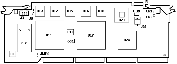
C39 22uF capacitor
not present on P complex. Possible power filter?
CR1-CR2 Diagnostic
LEDs. CR1 lights momentarily at the start of POST, then turns off, CR2
stays on during POST, then turns off..
J6
Present on some P60/P66 complexes. Function unknown
J3 Serial
port connector to operator panel board.
J5 Serial
Link Intended for use with an earlier system management adapter, which
didn't made it to the salesroom. The idea was to supply a sort of status-link
to the processorboard and the SCSI- adapter(s) and the (possible)
backplanes on the later servers.
JMP5 Flash
ROM bank switch originally planned for a sort of "emergency mode".
Once you screwed up the Flash-BIOS you could toggle the bank, insert any
working flash update in the FDD A: and restart the machine, which
takes the flash-image from the floppy drive and recovers (as it can be
done on the 704 in the "Bios recovery mode"). However: the base boot-BIOS
lacked the required routines to delete the loused up bank of the Flash-ROM
... and as far as I know the loading of an image from Floppy does
not work. Another useless feature.
OS1 66 MHz oscillator.
CPU Bus clock. You can replace a 60 with a 66 MHz osc.
U3
10G3407 Flash BIOS, Odd ?
U5
10G3372 Flash BIOS Even ?
U11
Socket 4 5v for Pentium 60 or 66
U13
87X0079
U17
A82496-66 Cache controller Try HERE
and search for A82496-66. Thanks, Senum!
It uses the
ten square black chips along the top edge. Those chips are 82491-66
U23
10G3441 SynchroStream
Controller Can be yellow or blue. Currently investigating if there
is any meaning to this difference as is the case with the 76/77 planars.
U24
50G8192 Unknown DMA Controller?
U25
Linear Technology LT1085CT Voltage Regulator
Outline Left of CPU
Unknown. Maybe for a component that used four mounting posts to match the
pattern. The right pair have thick PCB traces going to them. Maybe a VRM?
Q Complex Back
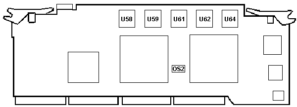
OS2 40 MHz MCA Bus Clock
Intel Pentium Overdrive
133MHz (POD133/120)
From Terminaut
I dug through craploads of old Intel documents today,
and found my notes from Intel (circa '95) for the Pentium Overdrive 133MHz
(POD133/120) processor.
Written in plain ingles, the Intel doc says: "will not
support the 82496 Cache Controller and 82491 Cache SRAM chip set"
Additionally, the documentation states that the POD133
is designed to support _PCI_ chipsets.
Some other notes:
- IU, IV, and IBT plus have been removed
- branch trace pins (BT[3:0]) have been removed (no execution
tracing)
- breakpoint pins (BP[3:0]) have been redefined such that each
assertion of one of these pins indicates that 1 to N BP matches occurred,
where N =core/bus frequency ratio
- STI/CLI (restore/clear interrupts) are each 2 clocks shorter
496 vs. 497 Cache
Controller
From Dr. Jim Shorney
Overdrive processors are not compatible with the '496
cache controller on the P60/66 complexes. However... I swapped
out the '496 cache controller on mine for a borrowed '497 (well heatsinked)
and was able to boot DOS with a POD 133 on my P60 (overclocked to 66).
It wasn't entirely stable, and would not boot OS/2 Warp 4.0 or NT 4.0.
The Powerleap PL54C interposer was still dead in this configuration.
There may yet be hope, I haven't tried the Powerleap with anything other
than an Intel 166 yet, and I may also downclock the complex back to 60
MHz and see what happens. There may yet be hope...
The '497 reportedly has a 3.3v core,
but it seemed to run stable and reliable for several hours with the stock
P60 CPU in my system in place of the 5v '496. I briefly looked
over the docs this afternoon (712 pages, wow...). Seems the '497 is still
a 5v part, it is the I/O buffers that connect to the CPU that are 3.3v.
This probably explains in part why the chip doesn't self-destruct in the
'496 socket. It also seems to invalidate the need for an interposer,
since the P60/66 I/O is 5v anyway and the buffers would have to run at
5v to interface at all with the CPU. This brings up the question
of noise immunity, though - will circuits designed to run at 3.3v logic
levels be more or less sensitive to noise or poor signal quality when run
at 5v? Inquiring minds want to know.
From Tony Ingenoso
I suspect noise is going to be less of a problem
at higher voltages Jim. In theory, the voltage range for correct
operation would be wider(particularly for CMOS). The only reason
I ever saw (other than laptop applications) for the drive to lower voltages
was to limit heat as the gate counts and frequencies went up. CMOS
parts like high voltages -- you can crank clock speeds faster with higher
voltages(the standard overclockers trick). Discrete type CMOS parts
can often be run as high as 20V and work fine. The downside is that
its power characteristics start approaching those of TTL at the higher
speeds (and heat goes up). If the only nominally 3.3V sections of
the cache controller are the line drivers/buffers, there's probably not
going to be enough stuff getting overvoltaged to make any significant difference
in the power draw.
9595 Server 95 (AKA "Server 95 566")
9595-0QT - P66, 16/256MB (ECC), 1GB SCSI-2 F/W, 2.88,
9595-0QTF - As above - Canadian French
9595-0QV - P66, 16/256MB (ECC), 2GB SCSI-2 F/W, 2.88
9595-PQG - Pentium 66, 16/256MB (ECC), 540MB SCSI-2 F/W, 2.88
9595-PQT - P66, 16/256MB (ECC), 1GB SCSI-2 F/W, 2.88
9595 Server 95 Array Models (Also called 95A)
9595-3QG - P66, 16/256MB (ECC), 3 x 540MB SCSI-2 F/W, 2.88
9595-3QT - P66, 16/256MB (ECC), 3 x 1GB SCSI-2 F/W, 2.88
NOTE: SERVER 95 -PQG &
-PQT models came with MGA Ultima Video Graphics Adapter, CD-ROM-II drive,
and 3-button mouse
9595
Main Page
|