MC/Xi Boards
@6FE9.ADF 4/8
ports, RS-232, 128K memory.
@6FEA.ADF
4/8 ports, RS-422, 128K memory.
@6FEB.ADF
16 ports, RS-232, 128K memory.
@7F99.ADF
4/8 ports, RS-232, 32K memory.
@7F9A.ADF
4/8 ports, RS-422, 32K memory.
@7F9B.ADF
16 ports, RS-232, 32K memory.
Drivers
For Legacy Digi Boards AIX, OS/2, Win, Unix (not Linux)
90029100B.pdf
Installation Guide (old 64K, Xe, MC/Xi, and COM/Xi).
92000161C.pdf
Software manual for OS/2 & Win3.x for PC/X and MC/X.
92000220C.pdf
Software manual for Win3.1x,95,NT for COM/Xi, Xe(MC),Xi(MC), Xem(MC),C/X(MC),EPC/X(MC)
4000312U.exe
MCA ADFs for Digi MC Products.
MC/Xi Processor Board with part number 30001224.
MC/8i
J1Dual Ported
Memory Window Size
J5-J6 (J3-J4 on RS-422/485
Boards)
EPROM
Size Jumpers (RS-232)
EPROM
Size Jumpers (RS-422, RS-422/RS-485)
Synchronous
Serial InterfaceMC/Xi+
MC/Xi+ (RS-232) Synchronous
Port Pin Assignments
MC/8i (optional
synchronous port shown)
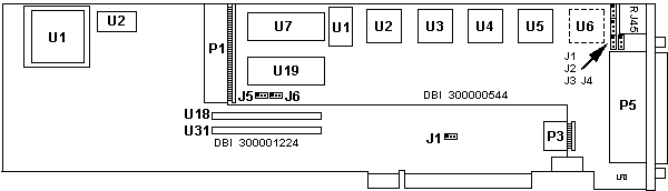
Processor Card
J1 Dual Ported
Memory Window
P1,3
U1 80C186-12
U2 25.000000 MHz osc
U18,31 MT4C1664Z-8 |
Daughter Card
J1-4 synchronous port function
J5,6 EPROM Size Jumpers
P5 DB78 Output
RJ-45 Xi+ synchronous port
U1 7.372800 MHz osc
U2-6 Zilog Z0853008VSC SCC
U7,19 BIOS |
This is board does not employ a daughtercard that makes a "sandwich"
when installed. The Processor Card ("Motherboard") contains the CPU, memory
and the MCA edgecard. The I/O Mate ("Daughtercard") has the BIOS, output
header, and the I/O controllers. It is the only card I've ever picked up
that "flexes". Odd...
MC/Xi refers to MC (Microchannel) and the number of ports, "X". So a
MC/8i would be an 8 port model.
J1Dual Ported
Memory Window Size
Jumper J1 determines whether the MC/Xi boards dual-ported
memory window size will be 32K or 128K. In most cases, if the board is
in a DOS machine, systems with 16MB or more of RAM, or systems with
a memory cache, the 32K window is recommended (factory default). This permits
the board to be installed with its memory window mapped into a 32K byte
range between 0C0000h and 0DFFFFh (below the 1MB boundary).
Installing the MC/Xi board below 1MB protects it from
interference from cache controllers on some MCA machines, and enables
the board to be installed in systems with 16MB of memory. If your system
has 12 MB or less of RAM, and the cache controller (if present) can be
disabled in the 13th through 16th megabyte, you can use the 128K setting,
thus freeing 32K of the 0C0000h-0DFFFFh address space for other expansion
boards which may not be addressable above 1MB.
J1 Settings
J5-J6 (J3-J4 on RS-422/485
Boards)
The MC/Xi I/O Mates have two jumpers, located near the EPROMs,
which identify the size of the EPROMs on the board. These jumpers are set
at the factory, and should only be changed if you are installing custom
EPROMs. On RS-232 versions of the MC/Xi, the jumpers are labeled J5 and
J6. On RS-422 and RS-422/RS-485 versions, they are J3 and J4.
MC/Xi EPROM
Size Jumpers (RS-232)
|
EPROM Size
|
J5 Pins
|
J6 Pins
|
|
*16K
|
1-2
|
1-2
|
|
32K
|
1-2
|
1-2
|
|
64K
|
1-2
|
2-3
|
|
128K
|
2-3
|
2-3
|
* The default EPROM size is 16K.
MC/Xi EPROM
Size Jumpers (RS-422, RS-422/RS-485)
|
EPROM Size
|
J5 Pins
|
J6 Pins
|
|
*16K
|
1-2
|
1-2
|
|
32K
|
1-2
|
1-2
|
|
64K
|
1-2
|
2-3
|
|
128K
|
2-3
|
2-3
|
* The default EPROM size is 16K.
Synchronous
Serial InterfaceMC/Xi+
A special version of the MC/Xi board, called the MC/Xi+
is available in four and eight-port configurations. The MC/Xi+ board has
a synchronous port in addition to the standard asynchronous ports.
The MC/Xi+ synchronous port uses a 10-pin RJ-45 jack located
above the DB-78 connector. Three of the ten pins are dual function pins,
set with jumpers J1-J4 . The table below shows the pin assignments for
the RJ-45 jack. Dual function pins also show the jumper settings required
for each function. Signals ending with A connect to the A port of the
8530 communications controller, and signals ending with B connect
to the B port of the 8530.
MC/Xi+ (RS-232) Synchronous
Port Pin Assignments
|
RJ-45
|
Signal Name
|
Jumpers
|
|
1
|
TRxCA Transmit/Receive Clock
|
J2 Pins 1-2
|
|
SYNB Synchronization B (RI)
|
J2 Pins 2-3
|
|
2
|
DSRA Data Set Ready A (Input)
|
J3 Pins 1-2; J4 Pins 1-2
|
|
SYNA Synchronization A (Output)
|
J3 Pins 2-3; J4 Pins 2-3
|
|
3
|
RTSA Request To Send A
|
|
|
4
|
GND
|
Chassis Ground
|
|
5
|
TxDA Transmitted Data A
|
|
|
6
|
RxDA Received Data A
|
|
|
7
|
SG Signal Ground
|
|
|
8
|
CTSA Clear To Send A
|
|
|
9
|
DTRB Data Terminal Ready B
|
|
|
10
|
RTxCA Receive/Transmit Clocks A
|
J1 Pins 1-2
|
|
DCDA Data Carrier Detect A
|
J1 Pins 2-3
|
9595 Main Page
|