8580 Planar Memory
IBM Planar Memory Cards
Pinout for IBM Planar Memory Cards
IBM Planar Memory
Cards
Pinout
for IBM Planar Memory Cards
David Beem insinuates:
Working on the presence detect for the Model 80
memory boards. Haven't seen the pinouts on any pages, even Fred's, which
has provided me some very good information.
The connector is 3 rows (A, B, & C) by 32 columns. These are marked
well, except for the 2Mb board. Put it chip-side down, connector at the
bottom. The solder pads for the connector on the circuit board now have
pin A1 in the lower lefthand corner, something like this:
Solder Side
C1 oooooooooooooooooooooooooooooooo C32
B1 oooooooooooooooooooooooooooooooo B32
A1 oooooooooooooooooooooooooooooooo A32
---------------------------------------------------
Connector
----------------------------------------------
We are mainly interested in pins A17 & A32, wired on all Model 80
types, & pins A16 & A18, N/Cs on the Type 1 planars, wired for
the Type 2 and 3 planars. An 'x' on the chart means the pin is tied to
ground.
A16 A17
A18 A32
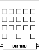
1Mb
x
x
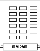
2Mb
x
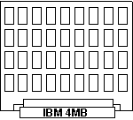
4Mb x x
x
This explains why the 4Mb modules are treated as 2Mb in
a Type 1 planar. I don't know if any of the presence detects signify memory
speed. The chart above shows the newer 2Mb board. Another surprise is the
little memory cards that go on the @FAFF.ADF 2 - 6Mb 386 Memory expansion
board are the same pinouts. Of course each board is 2Mb & the presence
detect is the same as above. I don't believe this board was offered in
any other capacity. You can use one of these little cards on the planar,
although it has to be in the slot furthest from the power supply due to
the keying & right-angle of the connector. At least the chips are conventional
& marked as 85nS.
Pinouts: (If all pinouts could be this simple; If all connectors wouldn't
be
this proprietary)
A1: Reserved
A2: -Mem Write
A3: Address 0
A4: Address 1
A5: Address 2
A6: Address 3
A7: Address 4
A8: Address 5
A9: Address 6
A10: Address 7
A11: Address 8
A12: -Row Address Strobe 0
A13: -Row Address Strobe 1
A14: -Row Address Strobe 2
A15: -Row Address Strobe 3
A16: Presence Detector (N/C on Type
1)
A17: Presence Detector
A18: Presence Detector (N/C on Type
1)
A19: -Column Address Strobe 0
A20: -Column Address Strobe 1
A21: -Column Address Strobe 2
A22: -Column Address Strobe 3
A23: Data Parity 0
A24: Data Parity 1
A25: Data Parity 2
A26: Data Parity 3
A27: -Byte Enable 0
A28: -Byte Enable 1
A29: -Byte Enable 2
A30: -Byte Enable 3
A31: -Column Address Strobe Parity
A32: Presence Detector |
B1: Ground
B2: +5VDC
B3: Ground
B4: +5VDC
B5: Ground
B6: +5VDC
B7: Ground
B8: +5VDC
B9: Ground
B10: +5VDC
B11: Ground
B12: +5VDC
B13: Ground
B14: +5VDC
B15: Ground
B16: +5VDC
B17: Ground
B18: +5VDC
B19: Ground
B20: +5VDC
B21: Ground
B22: +5VDC
B23: Ground
B24: +5VDC
B25: Ground
B26: +5VDC
B27: Ground
B28: +5VDC
B29: Ground
B30: +5VDC
B31: Ground
B32: +5VDC |
C1: Data 0
C2: Data 1
C3: Data 2
C4: Data 3
C5: Data 4
C6: Data 5
C7: Data 6
C8: Data 7
C9: Data 8
C10: Data 9
C11: Data 10
C12: Data 11
C13: Data 12
C14: Data 13
C15: Data 14
C16: Data 15
C17: Data 16
C18: Data 17
C19: Data 18
C20: Data 19
C21: Data 20
C22: Data 21
C23: Data 22
C24: Data 23
C25: Data 24
C26: Data 25
C27: Data 26
C28: Data 27
C29: Data 28
C30: Data 29
C31: Data 30
C32: Data 31 |
Peter Wendt shows a strong habit of too much time...
How about that comparison chart below ? I once made it
to build a
"Mod.80-to-72pin" converter - an attempt that failed so far, by various
reasons. (Lack of time mostly)
PIN-OUT COMPARISON CHART
IBM PS/2 Mod 80
IBM PS/2 Mod. 70
Memory Daughter Card
72-pin SIMM
A01 NA Reserved
A02 O -Memory Write
Write Enable O 47
A03 O -MA 0
Adress 0
O 12
A04 O -MA 1
Adress 1
O 13
A05 O -MA 2
Adress 2
O 14
A06 O -MA 3
Adress 3
O 15
A07 O -MA 4
Adress 4
O 16
A08 O -MA 5
Adress 5
O 17
A09 O -MA 6
Adress 6
O 18
A10 O -MA 7
Adress 7
O 28
A11 O -MA 8
Adress 8
O 31
A12 O -RAS 0
RAS 0
O 44
A13 O -RAS 1
RAS 1
O 45
A14 O -RAS 2
RAS 2
O 34
A15 O -RAS 3
RAS 3
O 33
A16 O -RAMHS (Type 3) 1
A17 O -R (Mod. inst.) 2
A18 O T2
(Type 3) 3
A19 O -CAS 0
CAS 0
O 40
A20 O -CAS 1
CAS 1
O 43
A21 O -CAS 2
CAS 2
O 41
A22 O -CAS 3
CAS 3
O 42
A23 IO -MPD 0
Parity Data 0 IO 36
A24 IO -MPD 1
Parity Data 1 IO 37
A25 IO -MPD 2
Parity Data 2 IO 35
A26 IO -MPD 3
Parity Data 3 IO 38
A27 O -BE 0
Block Select 0 O 29
A28 O -BE 1
Block Select 1 O 46
A29 O -BE 2
Block Select 2 O 66
A30 O -BE 3
Block Select 3 O 71
A31 O -CASP
-CAS P
O 11
A32 O T1 (Mod. Size) 4
B01 NA Ground
Ground
NA 1
B02 O +5VDC
+5VDC
O 10
B03 NA Ground
Ground
NA 39
B04 O +5VDC
+5VDC
O 30
B05 NA Ground
Ground
NA 72
B06 O +5VDC
+5VDC
O 59
B07 NA Ground
B08 O +5VDC
B09 NA Ground
B10 O +5VDC
B11 NA Ground
B12 O +5VDC
B13 NA Ground
B14 O +5VDC
B15 NA Ground
B16 O +5VDC
B17 NA Ground
B18 O +5VDC
B19 NA Ground
B20 O +5VDC
B21 NA Ground
B22 O +5VDC
B23 NA Ground
B24 O +5VDC
B25 NA Ground
B26 O +5VDC
B27 NA Ground
B28 O +5VDC
B29 NA Ground
B30 O +5VDC
B31 NA Ground
B32 O +5VDC
C01 IO Data 00
Data 00
IO 2
C02 IO Data 01
Data 01
IO 4
C03 IO Data 02
Data 02
IO 6
C04 IO Data 03
Data 03
IO 8
C05 IO Data 04
Data 04
IO 20
C06 IO Data 05
Data 05
IO 22
C07 IO Data 06
Data 06
IO 24
C08 IO Data 07
Data 07
IO 26
C09 IO Data 08
Data 08
IO 49
C10 IO Data 09
Data 09
IO 51
C11 IO Data 10
Data 10
IO 53
C12 IO Data 11
Data 11
IO 55
C13 IO Data 12
Data 12
IO 57
C14 IO Data 13
Data 13
IO 61
C15 IO Data 14
Data 14
IO 63
C16 IO Data 15
Data 15
IO 65
C17 IO Data 16
Data 16
IO 3
C18 IO Data 17
Data 17
IO 5
C19 IO Data 18
Data 18
IO 7
C20 IO Data 19
Data 19
IO 9
C21 IO Data 20
Data 20
IO 21
C22 IO Data 21
Data 21
IO 23
C23 IO Data 22
Data 22
IO 25
C24 IO Data 23
Data 23
IO 27
C25 IO Data 24
Data 24
IO 50
C26 IO Data 25
Data 25
IO 52
C27 IO Data 26
Data 26
IO 54
C28 IO Data 27
Data 27
IO 56
C29 IO Data 28
Data 28
IO 58
C30 IO Data 29
Data 29
IO 60
C31 IO Data 30
Data 30
IO 62
C32 IO Data 31
Data 31
IO 64
Reserved NA
19
Reserved NA
32
Reserved NA
48
PD 0
I 67
PD 1
I 68
PD 2
I 69
PD 3
I 70
Notes:
#1) Contact is tied to GND if the module
is High Speed (80ns)
#2) Contact is tied to GND to signal
installed module
#3) If T1=NC and T2=GND the module is
4MB (25MHz-boards only)
#4) If T1=GND and R=GND the module is
1MB (16MHz boards only)
If T1=NC and
R=GND there is a 2MB module installed (20Mhz only)
T2 is not present
on 16 & 20MHz platforms and may not be used
PS/2 Model 80 Presence Detection - Possible
Combinations
+--+---+---+--------------------------------------------+
R T1 T2 Module Presence / Type Pins
+--+---+---+--------------------------------------------+
NC X X No module present
in
G G X 1MB module
installed (16MHz planar)
G NC X 2MB module installed
(20MHz planar)
G NC G 4MB module installed
(25MHz planar)
+--+---+---+--------------------------------------------+
PS/2 Model 70 Presence Detection - Possible
Combinations
7 6 6 6
0 9 8 7 <---- Module Pins
+-+-+-+-+-------------------------------------------+
3 2 1 0 Presence Detect Value
+-+-+-+-+-------------------------------------------+
- - - - No module present (All
planars)
G G - G 1 MB / 100ns Parity (Type 1 planar
only)
G G G - 2 MB / 100ns Parity (Type 1 planar
only)
G - - G 1 MB / 85ns Parity (Type
1 + 2 planar)
G - G - 2 MB / 85ns Parity (Type
1 + 2 planar)
- G G - 2 MB / 80ns Parity (Type
3 + 4 planar)
+---+---+---+---+-----------------------------------+
R1 R2
<---- Memory coding on original IBM-modules
Type 1 are the full lenght 16 and 20MHz planars
Type 2 are the reduced lenght 16 and 20MHz planars
Type 3 is the 25MHz 386 planar
Type 4 is the 25MHz 486 planar
G = GND measured against Pin 72 (module GND)
- = open connection measured against Pin 72
9595 Main Page
|